


All Products
20 Layer Electronic Pcb Design Service Oem Odm Fabrication Prototype


| Place of Origin | China |
|---|---|
| Brand Name | CRT |
| Certification | ISO9001/ISO14001/IATF16949 |
| Model Number | CRT-SJ-008 |
| Minimum Order Quantity | 1piece |
| Price | US$ 1.18~2.73/piece |
| Packaging Details | Vacuum Packaging + Moisture + Humidity Card |
| Delivery Time | 14 working days |
| Payment Terms | T/T |
| Supply Ability | 40000sqm/month |
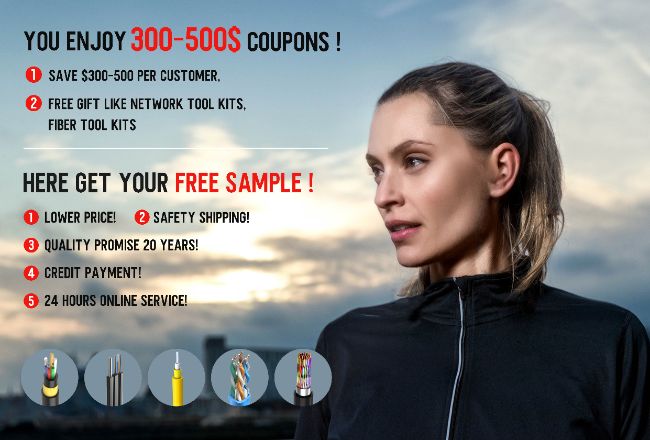
Contact me for free samples and coupons.
Whatsapp:0086 18588475571
Wechat: 0086 18588475571
Skype: sales10@aixton.com
If you have any concern, we provide 24-hour online help.
xProduct Details
| Application Segment | Auto, Industrial, Medical, DataCom, Camera | Layer Count | 1~20L |
|---|---|---|---|
| Matierial | PI, PET, PEN, FR4 | Board Thickness | 0.05mm~1.0mm |
| Copper Thickness | 0.33oz~5oz | Size | 2mm~1600mm |
| Highlight | 20 layer pcb design service,prototype pcb design service,oem electronic pcb design |
||
Product Description
Reliable High Quality OEM ODM PCB Design Fabrication Prototype Service
Why Choose Us:
1. Rich experience in PCB fabrication area: 90% engineers with nearly 20 years experience.
2. Safe and reliable test equipment: strict quality control, each process is optimized for the
3. Scientific quality control: comply with ISO operating procedures, focus on small to large volume production
4. Good quality traceability system: control in advance, existing quality problems are summarized and optimized in time
Specifications:
|
|||||||||||||||||||||||||||||||
FAQ:
Q1. Can I have a sample order to test it?
A: Yes, we welcome sample order to test and check quality. Mixed samples are acceptable.
Q2. What about the lead time?
A: Sample needs 3-5 days, mass production time needs 8-12 days.
Q3. Do you have MOQ for all PCBs?
A: NO MOQ,we do custom made PCB, and flexible PCB, depends on customers' projects.
Q4. How do you ship the goods and how long does it take to arrive?
A: For small quantity, we ship it by DHL, UPS, FedEx or TNT. It usually takes 3-5 days, and for big quantity needs 20-30 days by sea( the detail will be confirmed with the forwarder).
Q5. I have no drawing, how to process it?
A: First, let us know your detail requirements( if you have sample, please ship to us, we will copy it). Second, we quote according to your requirements or our suggestions. Third, customer confirms the samples and places deposit for formal order. Fourth, we arrange the production.
Q6. Is it OK to print my logo on product?
A: Yes. Please inform us formally before our production and confirm the design firstly based on our sample.
Q7: Do you offer guarantee for the products?
A: Yes, we offer 1-3 years warranty to our products.
Q8: How to deal with the faulty?
A: First, our products are produced in strict quality control system and the defective rate will be less than 0.1%. Second, during the guarantee period, if it's our fault, we will repair them and resend to you or we can discuss the detail, and find the final solution.
Picture Details:
Recommended Products